
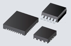


Texas Instruments CDCBT1001 Clock Buffer & Level Translator
Texas Instruments CDCBT1001 Clock Buffer and Level Translator is a 1.2V to 1.8V clock buffer and level translator for personal electronics, servers, and add-in cards. The VDD_IN pin supply voltage defines the input LVCMOS clock level. The VDD_OUT pin supply voltage defines the output LVCMOS clock level. VDD_IN = 1.2V ±10%. VDD_OUT = 1.8V ±10%. The 12kHz to 5MHz additive RMS jitter at 24MHz of the Texas Instruments CDCBT1001 is less than 0.8ps.
Features
- DC to 24MHz clock frequency range
- 1.2V to 1.8V LVCMOS clock level translation
- VDD_IN = 1.2V ± 10%
- VDD_OUT = 1.8V ± 10%
- Low additive jitter and phase noise
- 0.8ps maximum 12kHz to 5MHz additive RMS jitter (fout = 24MHz)
- –120dBc/Hz maximum phase noise at 1kHz offset (fout = 24MHz)
- –148dBc/Hz maximum phase noise floor (fout = 24MHz, foffset ≥ 1MHz)
- 5ns 20% to 80% rise/fall time
- 10ns propagation delay
- Low current consumption
- –40°C to 85°C operating temperature range
Applications
- FPGA/processor clock buffering/level translation in personal electronics
- 1.2V clock buffer and level translator in servers and add-in cards
Functional Block Diagram

Related Development Tool

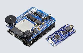
Texas Instruments CDCBT1001EVM Evaluation Module (EVM)
Item is designed to evaluate the CDCBT1001, a 1.2V to 1.8V clock buffer and level translator.
Published: 2022-06-21
| Updated: 2022-07-04