


Texas Instruments AM261x/AM261x-Q1 Arm®-Based Microcontrollers

Texas Instruments AM261x/AM261x-Q1 Arm®-Based Microcontrollers are designed to meet the complex real-time processing needs of next-generation industrial and automotive embedded products. With scalable Arm Cortex®-R5F performance and an extensive set of peripherals, the Texas Instruments AM261x/AM261x-Q1 device is designed for a broad range of applications while offering safety features and optimized peripherals for real-time control. The AM261x-Q1 device is AEC-Q100 qualified for automotive applications.
Features
- Processor cores
- Single and dual Arm Cortex-R5F CPU with each core running up to 500MHz
- 16KB I-cache with 64-bit ECC per CPU core
- 16KB D-cache with 32-bit ECC per CPU core
- 256KB Tightly Coupled Memory (TCM) with 32-bit ECC per core
- Lockstep or dual-core operation supported
- Trigonometric Math Unit (TMU) for accelerating trigonometric functions with up to 2x, one per R5F MCU core
- Single and dual Arm Cortex-R5F CPU with each core running up to 500MHz
- Memory
- 1.5MB of On-Chip Shared RAM (OCSRAM)
- Three banks × 512KB
- ECC error protection for full 1.5MB OCSRAM
- Remote L2 Cache (RL2) for external memory, software programmable up to 256KB per CPU core
- 2x Octal Serial Peripheral Interface (OSPI) up to 133MHz SDR and DDR
- 1x with eXecute In Place (XIP) support
- RAM expansion/Flash over the Air (FOTA)
- General-Purpose Memory Controller (GPMC)
- 16-bit parallel data bus with 22-bit address bus and four chip selects
- Up to 4MB addressable memory space
- Integrated Error Location Module (ELM) support for error checking
- 1.5MB of On-Chip Shared RAM (OCSRAM)
- System on Chip (SoC) services and architecture
- 1x EDMA to support data movement functions
- The following interfaces support Device Boot
- UART (primary/backup)
- OSPI NOR and NAND Flash (50MHz SDR and 25MHz DDR) (primary)
- USB peripheral boot
- Interprocessor communication modules
- SPINLOCK module for synchronizing processes running on multiple cores
- MAILBOX functionality implemented through the CTRLMMR registers
- Central Platform Time Sync (CPTS) support with time-sync and compare-event interrupt routers
- Timer modules
- 2x Windowed Watchdog Timer (WWDT)
- 4x Real-Time Interrupt (RTI) timer
- USB 2.0
- Port configurable as USB host, USB device, or USB dual-role device
- USB 2.0 host mode
- High-Speed (HS, 480Mbps)
- Full-Speed (FS, 12Mbps)
- Low-Speed (LS, 1.5Mbps)
- USB 2.0 device mode
- High-Speed (HS, 480Mbps)
- Full-Speed (FS, 12Mbps)
- Industrial connectivity
- 2x Programmable Real-time Unit – Industrial Communication Subsystem (PRU-ICSS)
- Dual-core Programmable Realtime Unit Subsystem (PRU0 / PRU1) per PRU-ICSS for 4 cores total
- Deterministic hardware
- Dynamic firmware
- 20-channel enhanced input (eGPI) per PRU
- 20-channel enhanced output (eGPO) per PRU
- Embedded Peripherals and Memory
- 1x UART, 1x ECAP, 1x MDIO, 1x IEP
- 1x 32KB Shared General Purpose RAM
- 2x 8KB Shared Data RAM
- 1x 12KB IRAM per PRU
- ScratchPad (SPAD), MAC/CRC
- Digital encoder and sigma-delta control loops
- The PRU-ICSS enables advanced industrial protocols, including:
- EtherCAT®, Ethernet/IP™
- PROFINET®, IO-Link®
- Dedicated Interrupt Controller (INTC)
- Dynamic CONTROLSS XBAR integration
- Dual-core Programmable Realtime Unit Subsystem (PRU0 / PRU1) per PRU-ICSS for 4 cores total
- 2x Programmable Real-time Unit – Industrial Communication Subsystem (PRU-ICSS)
- High-speed interfaces
- Integrated 3-port gigabit Ethernet switch (CPSW) supporting up to two external ports
- Selectable MII (10/100), RMII (10/100), or RGMII (10/100/1000)
- IEEE 1588 (2008 Annex D, Annex E, Annex F) with 802.1AS PTP
- Clause 45 MDIO PHY management
- 512x ALE engine-based packet classifiers
- Priority flow control with up to 2KB packet size
- Four CPU hardware interrupt pacing
- IP/ UDP/ TCP checksum offload in hardware
- Time Sensitive Network (TSN) support
- Cut-thru switching and Interexpress Traffic (IET) support
- Integrated 3-port gigabit Ethernet switch (CPSW) supporting up to two external ports
- General connectivity
- 6x Universal Asynchronous RX-TX (UART)
- 4x Serial Peripheral Interface (SPI) controllers
- 3x Local Interconnect Network (LIN) ports
- 3x Inter-Integrated Circuit (I2C) ports
- 2x Modular Controller Area Network (MCAN) modules with CAN-FD support
- 1x Fast Serial Interface Transmitter (FSITX)
- 1x Fast Serial Interface Receiver (FSIRX)
- Up to 141x General Purpose I/O (GPIO) pins
- Sensing and actuation
- Real-time Control Subsystem (CONTROLSS)
- Flexible Input/Output Crossbars (XBAR)
- 3x 12-bit Analog to Digital Converters (ADC) with 3 MSPS maximum sampling rate
- Each ADC module with
- 7x single-ended channels OR
- 3x differential channels
- Highly configurable ADC digital logic
- With selectable internal or external reference
- 4x post-processing blocks for each ADC module
- Each ADC module with
- 9x analog comparators with internal 12-bit DAC reference (CMPSSA)
- 1x 12-bit Digital to Analog Converter (DAC)
- 10x Enhanced High-Resolution Pulse Width Modulation (eHRPWM) modules
- Single or dual PWM channels
- Advanced PWM configurations
- Enhanced HRPWM time resolution
- 8x Enhanced Capture (ECAP) modules
- 2x Enhanced Quadrature Encoder Pulse (EQEP) modules
- 2x Sigma-Delta Filter Modules (SDFM)
- Data storage of 1 × 4-bit Multi-Media Card/Secure Digital (MMC/SD) interface
- Security
- Hardware Security Module (HSM) with support for Auto SHE 1.1/EVITA
- Targeted for ISO 21434 compliance
- Secure boot support
- Device takeover protection
- Hardware-enforced root-of-trust
- Authenticated boot
- SW anti-rollback protection
- Debug security
- Secure device debug only after proper authentication
- Ability to disable device debug functionality
- Device ID and key management
- Support for OTP memory (FUSEROM)
- Store root keys and other security fields
- Separate EFUSE controllers and FUSE ROMs
- Unique device public identifiers
- Support for OTP memory (FUSEROM)
- Memory Protection Units (MPU)
- Dedicated Arm MPU per Cortex-R5F core
- System MPU - present at various interfaces in the SoC (MPU or firewall)
- 8 to 16 programmable regions
- Enable/privilege ID
- Start/end address
- Read/write/cacheable
- Secure/non-secure
- Cryptographic acceleration
- Cryptographic cores with DMA support
- AES-128/192/256-bit key sizes
- SHA2-256/384/512-bit support
- DRBG with pseudo and true random number generator
- Functional safety
- Enables the design of systems with functional safety requirements
- Error Signaling Module (ESM)
- ECC or parity in the calculation of critical memories
- Built-In Self-Test (BIST) on-chip RAM
- Runtime internal diagnostic modules, including voltage, temperature, and clock monitoring, windowed watchdog timers, and CRC engines for memory integrity checks
- Functional safety-compliant targeted [industrial]
- Developed for functional safety applications
- Documentation to be made available to aid the IEC 61508 functional safety system design
- Systematic capability up to SIL-3 targeted
- Hardware integrity up to SIL-3 targeted
- Safety-related certification - IEC 61508 planned
- Functional safety-compliant targeted [automotive]
- Developed for functional safety applications
- Documentation to be made available to aid ISO 26262 functional safety system design
- Systematic capability up to ASIL-D targeted
- Hardware integrity up to ASIL-D targeted
- Safety-related certification - ISO 26262 planned
- Enables the design of systems with functional safety requirements
- Technology / Package
- AEC-Q100 qualified for automotive applications
- ZCZ package
- 324-pin NFBGAs
- 15.00mm × 15.00mm
- 0.8mm pitch
- ZFG package
- 304-pin NFBGA
- 13.25mm × 13.25mm
- 0.65mm pitch
- ZEJ package
- 256-pin NFBGA
- 13.00mm × 13.00mm
- 0.8mm pitch
- ZNC package
- 293-pin NFBGA
- 10.00mm × 10.00mm
- 0.5mm pitch
Applications
- AC inverter
- Automotive digital power conversion/control
- Battery Management Systems (BMS)
- On-board chargers, DC/DC converters
- Humanoid robot
- Industrial and collaborative robots
- Industrial digital power control
- Energy storage systems
- EV charging
- String inverters
- Mobile robot
- PLC, DCS, and PAC
- Communication module
- Digital input module
- Digital output module
- Stand-alone remote IO
- Remote I/O
- Single and multi-axis servo drives
- Telematics control unit
Functional Block Diagram

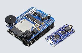
Development Tools
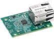
Texas Instruments DP83826-EVM-AM2 Evaluation Module (EVM)
Ethernet PHY add-on board for AM2x series Arm-based high-performance MCU evaluation modules.
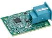
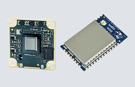
Texas Instruments DP83TG720-EVM-AM2 Evaluation Module (EVM)
Ethernet PHY add-on board for AM2x series Arm®-Based high-performance MCU evaluation modules.

Texas Instruments TMDSEMU560V2STM-UE XDS560v2 System Trace
Debug probes that support both the traditional JTAG standard (IEEE1149.1) and cJTAG (IEEE1149.7).