
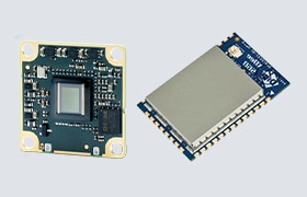
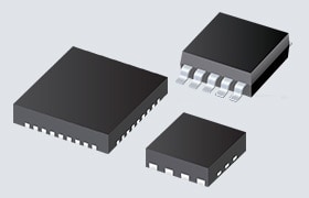


Texas Instruments LMK3H0102/LMK3H0102-Q1 Clock Generators
Texas Instruments LMK3H0102/LMK3H0102-Q1 Referenceless Clock Generators are two-output PCIe Gen 1 to Gen 6 compliant reference-less clock generators with Spread Spectrum Clocking (SSC) support. These are based on TI's proprietary Bulk Acoustic Wave (BAW) technology and provide ±25ppm clock outputs without any crystal or external clock reference. These devices can provide two SSC clocks, two non-SSC clocks, or one SSC clock and one non-SSC clock simultaneously. The LMK3H0102/LMK3H0102-Q1 meets the full PCIe compliance from Gen 1 to Gen 6. This compliance includes Common Clock with or without SSC, Separate Reference Independent Spread (SRIS), and Separate Reference No Spread (SRNS). These devices can be easily configured through GPIO pins or an I2C interface. An external DC-DC can be used to power the devices. The LMK3H0102-Q1 devices are AEC-Q100 qualified for automotive applications.
Features
- Integrated BAW resonator, no need for external reference
- Flexible frequency generation
- Two-channel dividers with up to three unique output frequencies from 2.5MHz to 400MHz
- LVCMOS outputs of 1.8V, 2.5V, or 3.3V are supported up to 200MHz
- Combination of AC-LVDS, DC-LVDS, LP-HCSL, and LVCMOS on OUT0 and OUT1 pins
- Additional LVCMOS output for the generation of up to five LVCMOS clocks
- Very low PCIe jitter with SSC
- PCIe Gen 3 Common Clock jitter: 135.3fs maximum (PCIe limit is 1ps)
- PCIe Gen 4 Common Clock jitter: 135.3fs maximum (PCIe limit is 500fs)
- PCIe Gen 5 Common Clock jitter: 57.5fs maximum (PCIe limit is 150fs)
- PCIe Gen 6 Common Clock jitter: 34.5fs maximum (PCIe limit is 100fs)
- PCIe Gen 1 to Gen 6 compliant with Common Clock with or without SSC, SRNS, and SRIS
- Total output frequency stability of ±25ppm
- Two functional modes (I2C or preprogrammed OTP) with a fully configurable I2C address
- –40°C to 85°C ambient temperature
- Programmable SSC modulation depth
- Preprogrammed: –0.1%, –0.25%, –0.3%, and –0.5% down spread
- Register programmable: –0.1% to –3% down spread or ±0.05% to ±1.5% center spread
- 1.8V to 3.3V supply voltage
- Internal LDOs with –93.1dBc PSNR at 500kHz switching noise for LP-HCSL outputs
- Start-up time of < 1.5ms
- Output-to-output skew of < 50ps
- Fail-safe digital input pins
Applications
- PCIe Gen 1 to Gen 6 clock generation
- Server motherboard
- NIC, SmartNIC
- Hardware accelerator
- Multifunction printer
- PCIe SSD
- Add-in card, PCIe expansion card
Datasheets
Functional Block Diagram

Related Development Tool
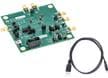
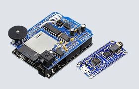
Texas Instruments LMK3H0102EVM Evaluation Module (EVM)
Evaluates clock performance, pin configuration, software configuration & features of the LMK3H0102.
Published: 2024-12-02
| Updated: 2025-07-10