
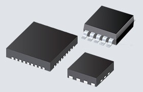


onsemi NVMFS5832NL Single N-Channel Power MOSFET

onsemi NVMFS5832NL Single N-Channel Power MOSFET is a high-performance MOSFET designed for low-voltage applications requiring efficient power switching. Built on advanced trench technology, the onsemi NVMFS5832NL offers an exceptionally low RDS(on) of 4.2mΩ at VGS = 10V, enabling reduced conduction losses and improved thermal performance. With a maximum drain-source voltage of 40V and a continuous drain current rating of up to 120A, this MOSFET is ideal for demanding environments such as DC-DC converters, synchronous rectification, and motor control. The compact 5mm x 6mm Power DFN package ensures high power density and excellent thermal dissipation, while the device’s low gate charge supports fast switching for enhanced efficiency in high-frequency designs.
Features
- 40V, 4.2mΩ, 120A device
- DFN5 (SO-8FL) Case 488AA Style 1 package
- Small footprint (5mm x 6mm) for compact designs
- Low RDS(on) to minimize conduction losses
- Low QG and capacitance to minimize driver losses
- Wettable flanks product
- AEC-Q101 qualified and PPAP capable
- Lead-free and RoHS-compliant
Applications
- Engine control modules
- Body control modules
- Chassis control modules
Specifications
- 40V maximum drain-to-source voltage
- ±20V maximum gate-to-source voltage
- 557A maximum pulsed drain current
- 120A maximum body diode source current
- 134mJ maximum single pulse drain-to-source avalanche energy
- Off characteristics
- 40V minimum drain-to-source breakdown voltage
- 34.2mV/°C typical drain-to-source breakdown voltage temperature coefficient
- 1µA to 100µA maximum zero gate voltage drain current range
- ±100nA maximum gate-to-source leakage current
- On characteristics
- 1.4V to 2.4V gate threshold voltage range
- 6.4mV/°C typical negative threshold temperature coefficient
- 4.2mΩ to 6.5mΩ maximum drain-to-source on resistance range
- 21S typical forward transconductance
- Typical capacitance
- 2700pF input
- 360pF output
- 250pF reverse transfer
- Typical charges
- 25nC to 51nC total gate charge range
- 2.0nC threshold gate charge
- 8.0nC gate-to-source
- 12.7nC gate-to-drain
- 3.2V typical plateau voltage
- Switching characteristics
- 13ns turn-on delay time
- 24ns rise time
- 27ns turn-off delay time
- 8.0ns fall time
- Drain-source diode characteristics
- 1.2V maximum forward diode voltage
- 28.6ns typical reverse recovery time
- 14ns typical charge time
- 14.5ns typical discharge time
- 23.4nC typical reverse recovery charge
- Thermal resistance
- 1.2°C/W junction-to-mounting board (top), steady state
- 40°C/W junction-to-ambient, steady state
- -55°C to +175°C operating junction temperature range
- +260°C maximum lead soldering temperature
Schematic

Related MOSFETs

onsemi N-Channel 40V & 60V Automotive Power MOSFETs
Available in 5mm x 6mm flat-lead and dual-cool packages ideal for compact and efficient designs.

onsemi NVMx & NVTx Power MOSFETs
AEC−Q101 Qualified MOSFETs offering compact and efficient solutions for automotive applications.