onsemi NTK3139P P-Channel Single Power MOSFET
onsemi NTK3139P P-Channel Single Power MOSFET is available in a compact SOT-723 package with built-in ESD protection. The SOT-723 package has a 44% smaller footprint and is 38% thinner than an SC-89 package. The drain-to-source voltage (VDSS) is rated at -20V and has a continuous drain current (ID) rating of -780mA (TA = +25°C). The onsemi NTK3139P features a low threshold level allowing for a 1.5V RDS(on) rating (VGS = 1.5V, ID = -100mA) of 0.95Ω (typical). The onsemi device can be operated at a low logic level gate drive. Typical applications include load/power switching, interfacing (logic switching), and battery management for ultra-small portable electronics.Features
- P-channel switch with low RDS(on)
- 44% smaller footprint and 38% thinner than SC-89
- Low threshold levels allowing 1.5V RDS(on) rating
- Operated at a low logic level gate drive
- Lead-free, Halogen-free/BFR-free, and RoHS-compliant
Applications
- Load/power switching
- Interfacing (logic switching)
- Battery management for ultra-small portable electronics
Specifications
- -20V drain-to-source voltage (VDSS)
- ±6V gate-to-source voltage (VGS)
- Continuous drain currents (ID) of -780mA (TA = +25°C), -570mA (TA = +85°C), -870mA (t <= 5s, TA = +25°C)
- Power dissipation (PD) of 450mW (TA = +25°C), 550mW (t <= 5s, TA = +25°C)
- -55°C to +150°C operating junction/storage temperature (TJ, Tstg) range
- -1.2A pulsed drain current (IDM) (tp = 10µs)
- +260°C lead temperature for soldering purposes (TL)
- Drain-to-source on resistance [RDS(on)]
- 0.38Ω (typ.) at VGS = -4.5V, ID = -780mA
- 0.52Ω (typ.) at VGS = -2.5V, ID = -660mA
- 0.70Ω (typ.) at VGS = -1.8V, ID = -100mA
- 0.95Ω (typ.) at VGS = -1.5V, ID = -100mA
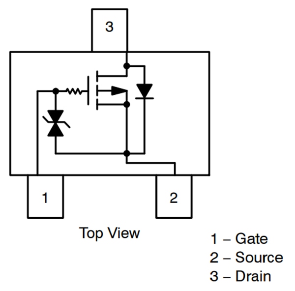
Circuit Diagram

Published: 2025-10-01
| Updated: 2025-10-14


