


onsemi NCP740 High Voltage Linear Regulators

onsemi NCP740 High Voltage Linear Regulators are designed to provide a compact, robust, and energy‑efficient solution for regulating high input voltages in industrial, telecom, and battery‑powered applications. The onsemi NCP740 supports a wide input voltage range from 3V up to 85V, while delivering up to 100mA of output current, making the regulators well-suited for systems powered from high‑voltage rails. The NCP740 devices are available in both fixed output versions (such as 3.3V) and an adjustable version ranging from 1.2V to 20V, with tight output accuracy of ±0.5% at +25°C.
The components feature ultra‑low quiescent current (typically 5µA), which helps extend battery life in low‑power designs, and the regulators remain stable with a small 1µF ceramic output capacitor, enabling reduced PCB area and simplified design. Integrated protection features (including thermal shutdown, current limiting, soft‑start to suppress inrush current, and undervoltage lockout [UVLO]) enhance system reliability under demanding conditions.
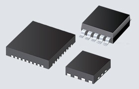
In addition, the onsemi NCP740 includes a power‑good (PG) output with a user‑programmable delay, implemented via an external capacitor, allowing designers to sequence downstream circuitry reliably. Housed in thermally enhanced MSOP‑8 EP and DFNW‑8 3mm × 3mm packages, the NCP740 combines high‑voltage tolerance, low power consumption, and comprehensive monitoring and protection features in a compact, lead‑free solution suitable for harsh and space‑constrained environments.
Features
- Wide 3V to 85V input voltage range
- Output voltage versions
- 3.3V fixed (other versions on request)
- Adjustable from 1.2V to 20.0V
- ±0.5% accuracy at TJ = +25°C
- Very low 5µA (typical) quiescent current
- 0.5µA typical standby current
- Stable with 1µF ceramic output capacitor
- Power good with programmable delay
- Thermal shutdown and current limit protection
- Built-in soft start circuit to suppress the inrush current
- Output active discharge functions
- Available in thermally enhanced MSOP8 EP and DFNW8 3mm x 3mm packages
- Lead-free and RoHS-compliant
Applications
- Telecom
- Industrial
- Battery and high-voltage rail sensors
- Alarms and security systems
- Battery-powered hand tools
- Home automation
- Smart metering
- White goods
Specifications
- Input
- 3V to 85V operating input voltage range
- 1.7V to 3.0V input voltage UVLO threshold range
- 0.01V to 0.5V input voltage UVLO hysteresis range
- Output
- ±1.5% maximum output voltage accuracy
- 1.2V typical ADJ reference voltage
- ±100nA ADJ input current
- 0.2% VOUT maximum line regulation
- 0.4% VOUT maximum load regulation
- 750mV maximum dropout voltage
- 110mA to 300mA output current limit range
- 110mA to 300mA short circuit current range
- 50Ω typical active discharge resistance
- Current consumption
- 5µA maximum disable current
- 15µA maximum quiescent current
- 500µA maximum ground current
- Enable thresholds
- 0.3V to 1.2V enable voltage threshold
- 0.01V to 0.3V enable voltage hysteresis
- 1µA maximum enable pin current
- 83µVRMS to 130µVRMS typical output noise voltage range
- Thermal shutdown
- +170°C typical temperature
- +15°C typical hysteresis
- +150°C maximum junction temperature
- +260°C maximum lead soldering temperature
- Thermal characteristics
- 35.4°C/W (DFNW-8) or 38.7°C/W (MSOP-8) junction-to-air thermal resistance
- 87.3°C/W (DFNW-8) or 102.0°C/W (MSOP-8) junction-to-case (top) thermal resistance
- 10.3°C/W (DFNW-8) or 14.7°C/W (MSOP-8) junction-to-case (bottom) thermal resistance
- 10.1°C/W (DFNW-8) or 15.2°C/W (MSOP-8) junction-to-board (top) thermal resistance
- 7.4°C/W (DFNW-8) or 10.3°C/W (MSOP-8) junction-to-case (top) thermal characterization parameter
- 10.2°C/W (DFNW-8) or 15.5°C/W (MSOP-8) junction-to-board (FEM) thermal characterization parameter
- Maximum ESD capability
- 2KV Human Body Model (HBM)
- 1kV Charged Device Model (CDM)
Typical Application Schematics

Internal Block Diagram
