


onsemi NCP3294 Stackable Synchronous Buck Regulator
onsemi NCP3294 Stackable Synchronous Buck Regulator is a highly efficient stackable synchronous buck regulator, capable of operating within an input range from 3V to 18V and supporting up to a 25A continuous load current. Higher output currents can be achieved by two parallel NCP3294 devices operating as an interleaved two-phase buck regulator. The onsemi NCP3294 utilizes fixed-frequency current-mode control to provide accurate voltage regulation and fast transient response. Flexible programming of functions and parameters supports multiple applications.
Features
- 3V to 18V input voltage (VIN) range with input feed-forward
- 0.5V to 5.5V output voltage (VOUT) range with remote output voltage sense
- 25A continuous output current, stackable to 50A
- Fixed frequency current mode control
- Integrated 5V LDO or external supply
- Enable with programmable VIN under-voltage lock-out (UVLO)
- Programmable boot-up voltage
- Programmable soft-start
- Pre-bias start-up
- Programmable current limit
- Power good indicator
- Selectable protection mode (latch-off or hiccup)
- Under-voltage and over-voltage protection
- Output discharge in shutdown
- +150°C operating junction temperature
- Moisture Sensitivity Level (MSL) 1
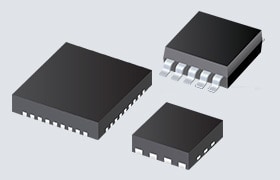
- WQFN34 package, 5mm x 7mm
- Lead-free and RoHS-compliant
Applications
- Networking (routers and switches)
- Telecom digital baseband
- Telecom radio units
- Server and desktop computers, notebooks, and gaming
- High-density power solutions
- DC-DC modules
- General-purpose POL regulators
Specifications
- 3V to 18V input range
- 0.5V to 5.5V output range
- 0A to 25A continuous output current range
- 200kHz to 2000kHz programmable switching frequency range, ±10% accuracy
- ±100mA maximum latch-up current rating, +150°C, per JEDEC JESD78
- -40°C to +150°C operating junction temperature range
- ESD
- 2kV minimum human body model per ANSI/ESDA/JEDEC JS-001
- 1.5kV minimum charge device model per ANSI/ESDA/JEDEC JS-002
- Thermal resistance
- 14.6°C/W junction-to-air
- 1.5°C/W MOSFET junction-to-PCB
Functional Block Diagram

Typical Application Circuits

Published: 2025-02-26
| Updated: 2025-03-11