


NXP Semiconductors FS6500 System Basis Chip
NXP Semiconductors FS6500 System Basis Chip (SBC) is a multi-output, SMARTMOS Power Supply Integrated Circuit (PMIC), featuring CAN FD (Controller Area Network Flexible Data) and/or LIN (Local Interconnect Network) transceivers. NXP FS6500 SBC provides power to MCUs and optimizes energy consumption through DC-DC switching regulators, linear regulators, and ultra-low-power-saving modes.
The FS6500 SBC includes configurable fail-safe/fail silent safety behavior and features, with two fail-safe outputs, becoming a full part of a safety oriented system partitioning, to reach a high integrity safety level (up to ASIL D). Multiple switching and linear voltage regulators, including a 32μA low-power mode, are available with various wake-up capabilities. An advanced power management scheme is implemented to maintain high efficiency over a wide range of input voltages down to 2.7V, and output current ranges up to 2.2A.
The built-in CAN FD interface fulfills the ISO 11898-2 (12) and -5(13) standards. The LIN interface fulfills LIN protocol specifications 2.0, 2.1(22), 2.2(23), and SAE J2602-2(24).
The FS6500/FS4500 feature configurable fail-safe/fail silent safety behavior, with two fail-safe outputs, becoming a full part of a safety-oriented system partitioning, to reach a high integrity safety level (up to ASIL B).
High-temperature capability up to TA = 125°C and TJ = 150°C, compliant with AECQ100 Grade 1 automotive qualification.
Features
- 2.7V up to 28V voltage operation range
- Buck pre-regulator with optional boost to fit with LV124 automotive test standards
- Ultra-low 30µA power modes
- Multiple wake-up sources in low-power mode: CAN, LIN, I/Os, LDT
- 3.3V keep alive memory supply available in low-power mode
- Independent fail-safe state machine supporting high functional safety standards
- Robust physical layers with superior EMI/ESD performance
- Five configurable I/Os
- 0.5A to 2.2A dual DC-DC supply
- Fail silent configurable safety architecture allowing independent monitoring of critical parameters and system availability
- System integration: analog multiplexer, battery sensing, long duration timer, and live memory supply to reduce BOM
- Scalable family, with a large range of pin-to-pin compatible part numbers supporting different system configurations for design flexibility
- Meets grade 0 reliability performance levels: qualified with 1300 hours of HTOL stress at Tj=+175°C
- 7mm x 7mm, 48-pin LQFP package, 0.5mm pitch
Applications
- Electric vehicles
- Hybrid electric vehicles
- Battery management systems
- Safety-critical motor control
- ADAS (advanced driver-assistance systems)
- Forward collision warning (FCW)
- Lane departure warning (LDW)
- Radar
- Sensor fusion safety area
- Drive train electrification
- Inverters
- DC-DC
- Alterno starters
- Drive train chassis and safety
- Active suspension
- Steering
- Safety domain gateways
- Functional safety integration
Brochures
Applications Infographic

Simple Block Diagram

Development Tools

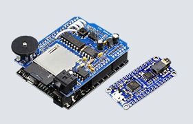
NXP Semiconductors FS6522 Freedom Evaluation Kit
Demonstration and evaluation platform for the MC33FS6522LAE System Basis Chip.

NXP Semiconductors FS6522 Evaluation Board
Easy-to-use platform for evaluating the FS6522 System Basis Chip.

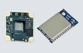
NXP Semiconductors RDVCU5775EVM Development Board
Features an MPC5775B MCU and provides a safe high-voltage battery management system (BMS) platform.

NXP Semiconductors MPC5775B-EVB & MPC5775E-EVB Development Boards
Features MPC5775B or MPC5775E MCU, silicon components, and interfaces for application development.

NXP Semiconductors RDGD3160I3PH5EVB HP Drive Reference Design
3-phase inverter reference design, based on GD3160 Gate Drivers, designed for HP Drive IGBT Modules.
NXP Semiconductors RDGD31603PHSEVM VE-Trac™ Drive Reference Design
3-phase inverter reference design, based on GD3160 Gate Drivers, designed for VE-Trac™ IGBT Modules.
Related Products

NXP Semiconductors PF5030 Fail-Safe System Basis Chip PMICs
Features a maximum input voltage of up to 5.25V and is designed for S32Z2/E2 processors.